Lab 02: Breadboard Computer Part 1#
In this lab, we will build a computer that can run a very simple C program:
int main(void) {
  while(1);
}
We will use an 8-bit data bus variant of the original Intel x86 processor known as the 80C88. A variant of this chip was used on the original IBM 5150 Personal Computer [4] and is still in production today [2].
Preliminaries#
Working with Hardware#
Hardware components can be delicate and easily damaged. This section offers a few basic tips for handling components.
Integrated Circuits#
The main components we will be using are called integrated circuits (ICs), which combine multiple logic gates onto a single silicon chip. The primary packaging we will be using for ICs is the dual inline package (DIP). These are made from plastic or ceramic and have a number of pins or legs coming out from the sides to make electrical connections.
Avoid touching the pins of a DIP with your fingers. This helps reduce the chance of discharging static electricity into one of these delicate chips. It also reduces the contamination of the pins, thus allowing for better electrical contact.
The pins can bend easily. Before inserting the DIP into a breadboard or socket, make sure that all pins are lined up. You will need to use some force to insert a DIP, but pay close attention to all the pins. If any seem like they are getting stuck, use a pair of tweezers to line things up before applying pressure.
Breadboards#
Breadboards are used to prototype circuits without soldering. They have a series of holes that are connected together in a specific pattern. The holes are used to insert wires and components to build a circuit.
There are two main types of connected holes on a breadboard: power rails and terminal strips. Power rails are used to distribute power to the circuit, while terminal strips are used to connect components together. Power rails run the entire length of the breadboard (all holes in a row are connected), while terminal strips are connected in groups of five. There is a gap between the rows of terminal strips to allow for DIPs to be inserted.
For this lab, we will be using a very large breadboard made up of several smaller breadboards connected together. We will use a three-dimensional coordinate system to describe the location of each hole on the breadboard. Take a look at the breadboard now:
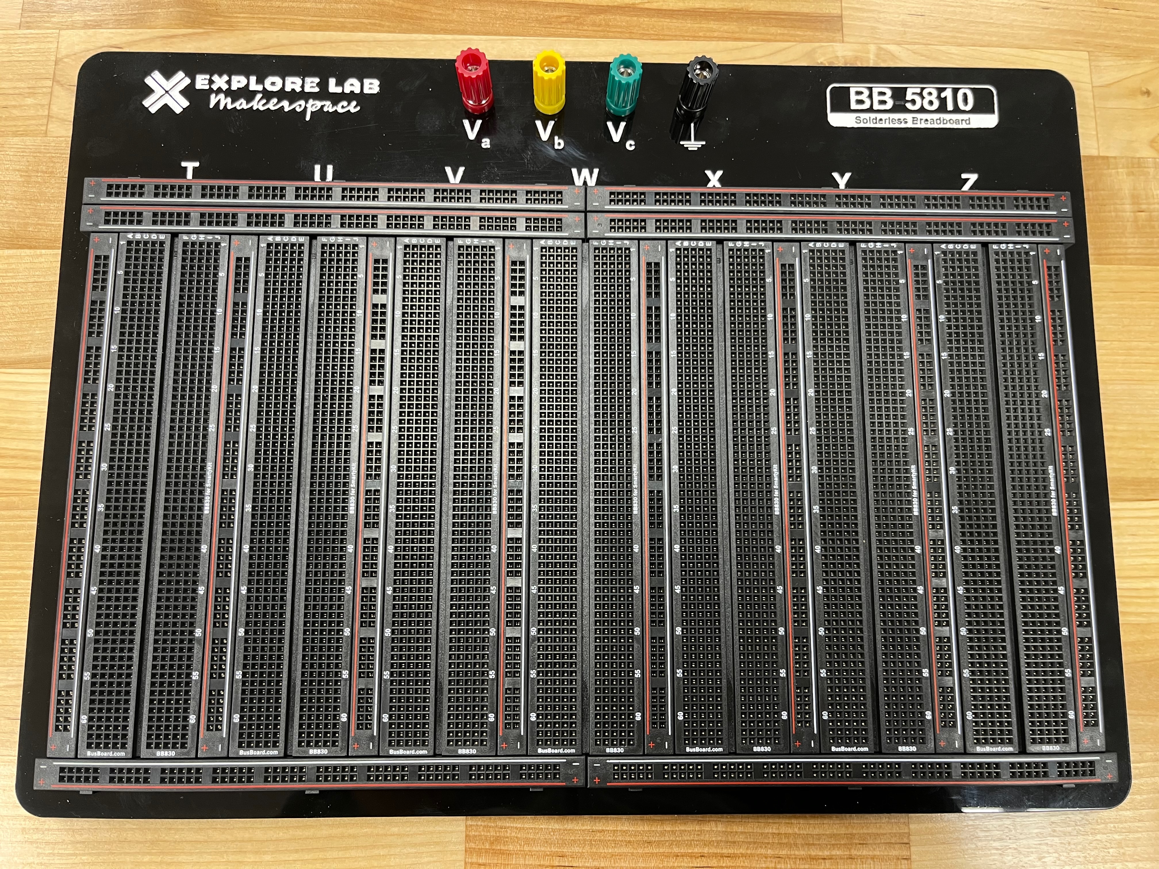
There are four binding posts on the breadboard. These are used to connect the power supply to the breadboard. The red binding post is for the positive voltage (or VCC), and the black binding post is for ground. The other two binding posts are not used in this lab, but can supply additional voltages.
The breadboard is divided into several sections identified by the letters printed on the board, U through Z. Each of these corresponds to an individual breadboard component. Each of these components had a numeric row value, 1 through 63. Finally, the columns in the row are identified by letters A through J, printed on the breadboard itself. Thus, we can identify a specific hole with a three-part coordinate, such as T-1-A. This is the hole in the upper-left corner of the breadboard.
Power Supplies#
The power supply is used to provide a stable voltage to the circuit. The power supply has two outputs: one for the positive voltage (VCC) and one for the ground. The power supply can be set to provide a specific voltage and current limit.

We use banana plugs to connect the outputs to the binding posts on the breadboard. The red banana plug is for the positive voltage, and the black banana plug is for the ground. The power supply has a power switch to turn the output on and off, and a display to show the voltage and current being supplied.
Connecting Wires#
You are provided with a variety of wires to connect components together. There should be enough to complete this lab, but you may need to request additional wires. There are four different lengths of wires used in this computer:
Extra Small (XS), which can connect holes at most three apart
Small (S), which can connect holes at most twelve apart
Medium (M), which can connect holes at most 45 apart
Long (L), which can connect holes at most 70 apart
There are six different colors of wires, which we use to indicate the kind of signal being carried:
Red: Power +5V (VCC) and Interrupts
Black: Ground (GND)
Blue: Control Signals
White: Address Signals
Green: Data Signals
Yellow: Clock Signals
Prepare for the lab#
Make sure that you have all the items needed for this lab:
Electrostatic foam with chips and passive components
12 0.1uF ceramic capacitors (marked 104)
1 100uF electrolytic capacitor
22 AWG hookup wire of lengths XS, S, and M
ZIF-28 to DIP-28 adapter
Bench Power Supply
2 Banana Wires
Breadboard
Tweezers
Chip Puller
You may wish to organize the wires by length and color to make them easier to find. Keeping things organized and tidy will help you work more efficiently.
The components on the electrostatic foam are organized so that you can easily find each item. You can reference the part number on the foam to the schematic diagrams in this lab to find the correct component. The component ID (unique for each element) is shown on the diagram of the foam below:

Before getting started, pick a name for your group and print out a label for your breadboard. Keep in mind, people will be able to see this name, so stay professional. (But you can have fun with it too!)
There will be a significant amount of reading to follow along with this lab. Details matter, so take your time and make sure you understand each step before moving on. If you have any questions, don’t hesitate to ask!
Within your group, make sure that everyone is participating. If one person is wiring up the computer, another could be reading off the steps and marking them as complete. A third person can then verify that wires have been connected correctly. Mistakes are bound to happen, and this will help you track everything.
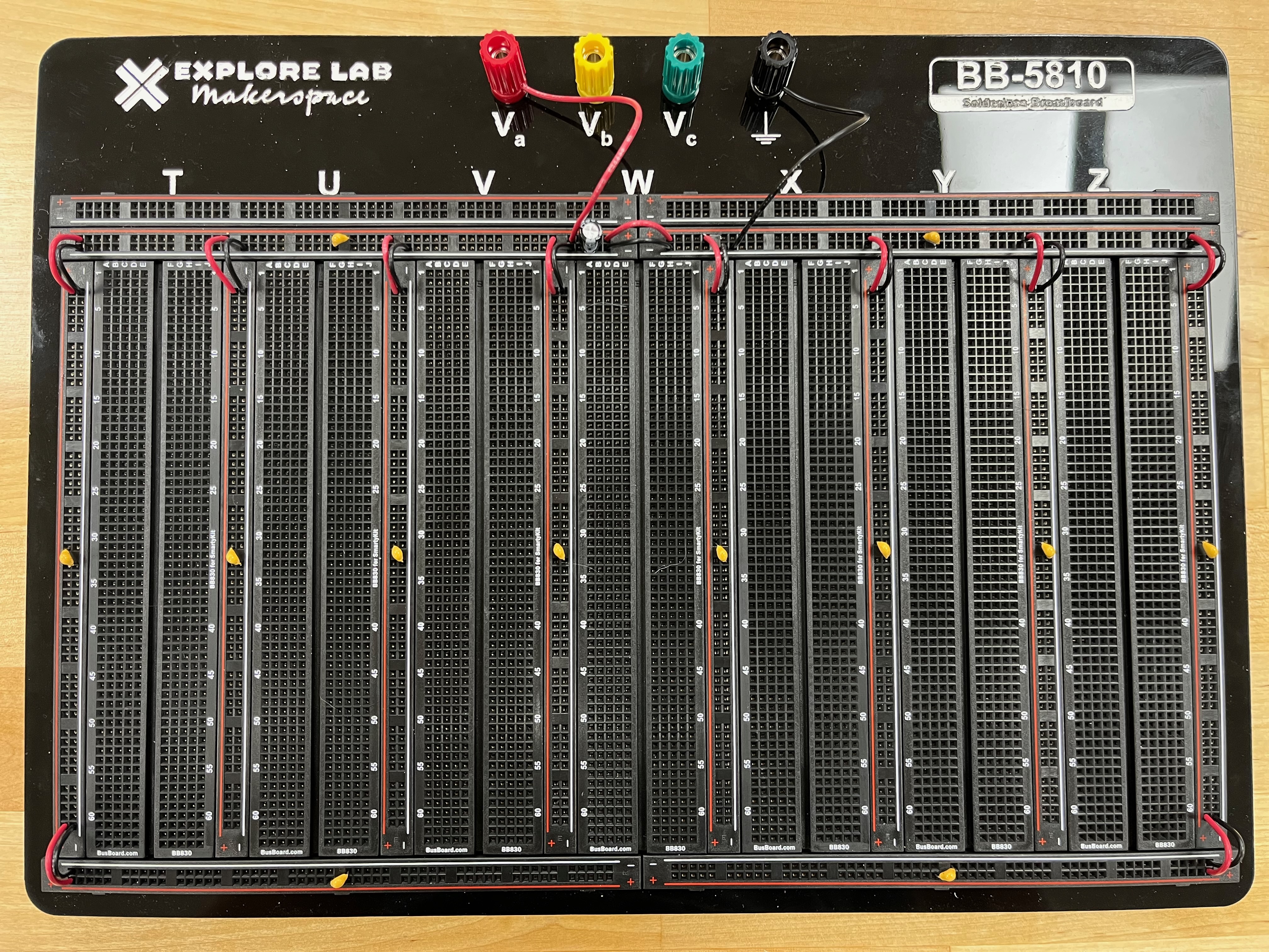
Step 1: Connect the Power Distribution Bus#
Note Leave the top power rail empty. We will use this to distribute other signals in the future.
Using 11 S red wires, connect the VCC (+) power bus rails (marked in red) together.
You do not need a jumper between the bottom two rails since they are connected via the vertical rails.
Using 11 S black wires, connect the GND (-) power bus rails (marked in white) together.
Partially unscrew the red binding post (Va) to reveal a mounting hole. Insert an M red wire into the hole (just the bare metal part), and tighten the binding post down. Insert the other end of the wire into the + power rail.
Repeat this process with an M black wire with the black binding post (ground).
Now, we will insert decoupling capacitors into the power rails. These help reduce the amount of AC signal on the power rails (recall: we want smooth DC supply).
Near where you plugged in the red binding post (near W-1-A), insert the 100uF electrolytic capacitor (it looks like a cylinder) into the + and - power rails. NOTE: the leg with the white stripe on the can must be inserted into the - power rail.
Insert one 0.1uF ceramic capacitor (brown blobs with 104 marked on the package) into the midpoint of each power rail between + and -. The orientation of these does not matter. The halfway point is near 32 on the vertical rails and U and Y on the horizontal rails.
Warning
Someone who did not wire the breadboard should now verify the above steps were completed correctly.
Your board should look similar to the following:
Test for Short Circuits#
A short circuit occurs when +5V (VCC) is connected to GND directly. This is bad. Before hooking in components, we will now verify there are no short circuits.
Plug the red banana wire from the + output on the power supply to the red binding post. Repeat the process with the black wire on the - output. Turn the power supply on with the power button. Verify that the supply is set to deliver 5V and limit current to 1A. It should look like the following before you start:
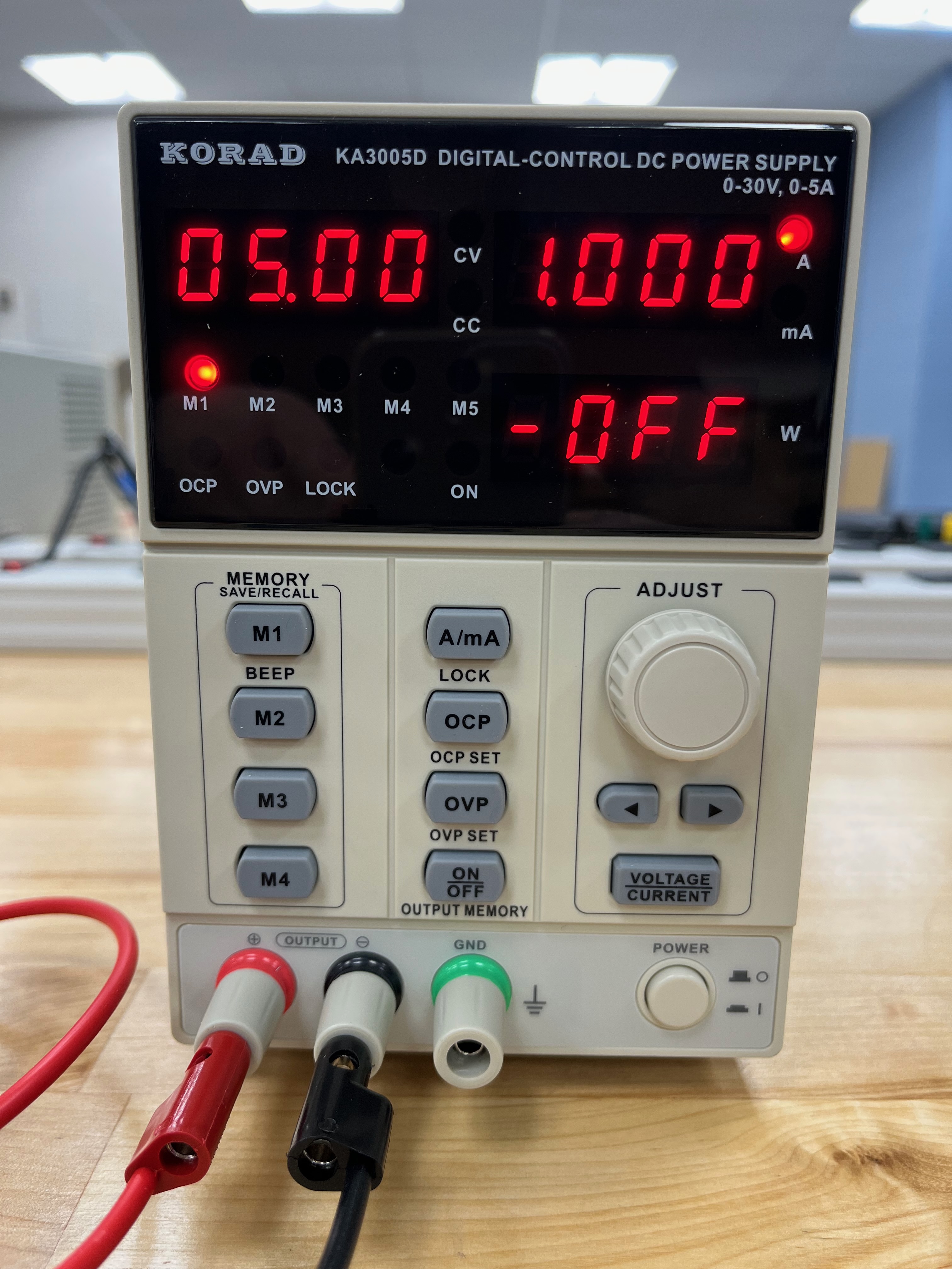
Press the ON/OFF button to turn on the power output. The green output light should come on, and the voltage should remain at 5V, but the current should drop to 0A.
If the opposite happens, you have mistake in your wiring. Press the ON/OFF button and go back to check your wiring!
Lab Report
Take a picture of your power rails and the power supply showing 0A of current.
Turn off the power supply output with the ON/OFF button and disconnect the banana plugs. It’s time to start building a computer!
Step 2: Clock Signal Generation#
Next, we will build a circuit to generate a clock signal. This signal will be used to synchronize the operation of the processor. The clock signal for the 80C88 will be 8MHz with a 33% duty cycle. This means that the signal will be high for 1/3 of the period and low for 2/3 of the period. The 82C84A chip is designed to generate this signal from a 24MHz crystal oscillator. It also generates the reset signal for the processor. We will also wire in a reset button to allow you to restart the computer without turning off the power.
We will be wiring up the schematic shown below.

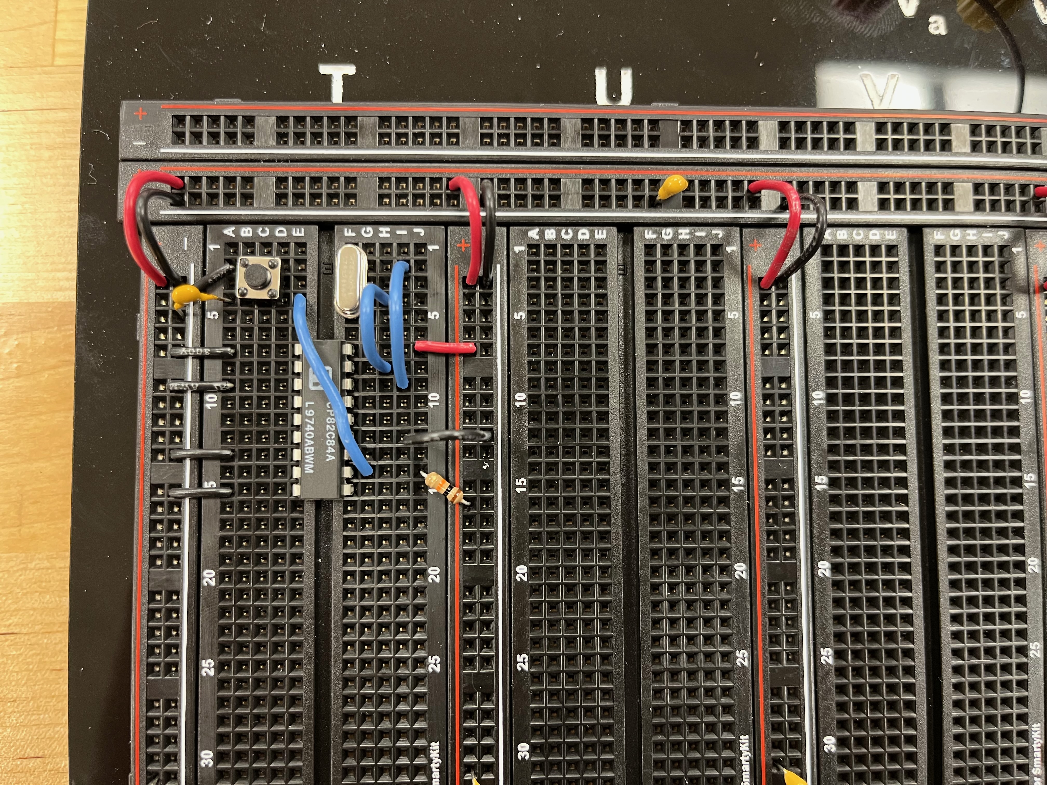
Wire up the Clock Circuit#
Insert the 24 MHz crystal (Y1) between T-2-F and T-4-F
Insert the pushbutton switch (SW1) between T-2-C and T-4-C
This is the reset switch
Connect T-2-A and GND with an XS black wire
Insert the 10 uF 106 ceramic capacitor (C1) between T-4-A and GND
Insert the 82C84A clock generator chip (U2) with pin 1 in T-7-E
The half-circle is at the top of the chip, and pin 1 is marked with a dimple
Insert the Brown-Black-Orange-Gold 10K resistor (R1) between T-14-J and VCC (diagonally near T-16-J)
Connect the following wires:
XS black: T-7-A — GND
XS black: T-9-A — GND
XS black: T-13-A — GND
XS black: T-15-A — GND
XS red: T-7-J — VCC
S black: T-12-J — GND
S blue: T-14-G — T-4-E
S blue: T-8-H — T-4-H
S blue: T-9-I — T-2-I
Note
You will see two S blue wires with the ends bent. These are useful for a later step in the build process. Use the straight ends for this step.
Your board should look similar to the following:
Warning
Someone who did not wire the breadboard should now verify the above steps were completed correctly.
Lab Report
Take a picture of your breadboard.
Check for Clock and Reset Signals#
Take your breadboard to the oscilloscope station
Plug in the VCC and GND supply wires
Connect the probes as follows
Yellow: VCC
Light Blue: T-14-A
Magenta: T-15-I
Dark Blue: T-14-I
Connect the grounds from the probes to ground
Press the
Singlebutton on the scopeThe screen should clear and the lights should turn green
Press ON/OFF on the power supply
You should now see four signals recorded, similar to the following:
Lab Report
Take a picture of the oscilloscope screen showing the clock signal.
Press the
Run/Stopbutton on the scopePress your reset button on the breadboard a couple of times and observe the behavior on the scope
Lab Report
Describe the behavior of the signals when you press the reset button. What four signals are you measuring?
Zoom in on the clock signal and measure the frequency. It should be 8MHz.
Lab Report
Take a picture of the oscilloscope screen showing the clock signal. Label the frequency measurement. Does this look like a square wave? Why or why not?
Press ON/OFF on the power supply
Disconnect all wires and return to your station
Step 3: Wire up Processor Logic#
Now, it is time to add the processor and associated supporting logic. The 80C88 shares some pins between data and address, so we will need latches to store the address while we read or write data. We will also need a buffer to drive the read and write output signals (along with some basic logic gates to decode this information). Finally, we need a bus transceiver to connect and disconnect the processor from the data bus.
We will be wiring up the schematic shown below. Note that the clock circuit you previously built is located in the upper left corner of this schematic.

Connect ICs and Power#
Insert the following ICs (make sure the pins are lined up before pressing firmly to fully seat the IC):
80C88-2 (U1) with pin 1 at T-20-D
74HCT245 Bus Transceiver (U3) with pin 1 at U-37-E
74HCT573 Latch (U4) with pin 1 at U-1-E
74HCT573 Latch (U5) with pin 1 at U-13-E
74HCT573 Latch (U6) with pin 1 at U-25-E
74HCT244 Buffer (U7) with pin 1 at U-50-E
74HCT04 Inverter (U8) with pin 1 at V-41-E
74HCT32 OR Gate (U10) with pin 1 at V-49-E
Connect the following power wires:
XS black: T-20-A — GND
XS black: T-36-A — GND
XS black: T-37-A — GND
XS black: T-39-A — GND
S black: T-29-J — GND
S black: T-37-J — GND
XS black: U-1-A — GND (top)
XS black: U-2-A — GND
XS black: U-3-A — GND
XS black: U-4-A — GND
XS black: U-5-A — GND
XS black: U-10-A — GND
XS black: U-13-A — GND
XS black: U-22-A — GND
XS black: U-25-A — GND
XS black: U-34-A — GND
XS black: U-46-A — GND
XS black: U-50-A — GND
XS black: U-59-A — GND
XS black: V-47-A — GND
XS black: V-55-A — GND
S black: U-51-J — GND
XS red: T-20-J — VCC
XS red: T-27-J — VCC
XS red: U-1-J — VCC (top)
XS red: U-13-J — VCC
XS red: U-25-J — VCC
XS red: U-37-J — VCC
XS red: U-50-J — VCC
XS red: V-41-J — VCC
XS red: V-49-J — VCC
Warning
Someone who did not wire the breadboard should now verify the above steps were completed correctly.
Lab Report
Take a picture of your breadboard. Label the chips on the board.
Connect Control, Address and Data#
Connect the following signal wires (blue):
S (bent ends): U-10-H — U-22-H
S (bent ends): U-22-G — U-34-G
S: V-50-B — V-53-A
S: T-33-J — U-37-A
M: T-11-D — T-38-I
M: T-15-G — T-39-I
M: T-35-J — U-34-H
M: T-34-J — U-38-G
M: T-32-J — V-50-A
M: T-31-J — V-52-A
M: T-28-J — V-49-A
M: U-51-A — V-51-A
M: U-52-A — V-54-A
Warning
Someone who did not wire the breadboard should now verify the above steps were completed correctly.
The breadboard should look similar to the following:
Note: The 74HCT245 is missing a GND wire in this image!
Lab Report
Take a picture of your breadboard.
Connect the following address wires (white):
M: T-21-I — U-14-A
M: T-22-I — U-9-A
M: T-23-I — U-8-A
M: T-24-I — U-7-A
M: T-25-I — U-6-A
M: T-21-C — U-15-A
M: T-22-C — U-16-A
M: T-23-C — U-17-A
M: T-24-C — U-18-A
M: T-25-C — U-19-A
M: T-26-C — U-20-A
M: T-27-C — U-21-A
M: T-28-C — U-26-A
M: T-29-C — U-27-A
M: T-30-C — U-28-A
M: T-31-C — U-29-A
M: T-32-C — U-30-A
M: T-33-C — U-31-A
M: T-34-C — U-32-A
M: T-35-C — U-33-A
Warning
Someone who did not wire the breadboard should now verify the above steps were completed correctly.
Connect the following data wires (green):
M: T-35-B — U-45-A
M: T-34-B — U-44-A
M: T-33-B — U-43-A
M: T-32-B — U-42-A
M: T-31-B — U-41-A
M: T-30-B — U-40-A
M: T-29-B — U-39-A
M: T-28-B — U-38-A
Warning
Someone who did not wire the breadboard should now verify the above steps were completed correctly.
Danger
Don’t miss the following step!
Finally, wire the clock signal to the processor (yellow):
M: T-14-D — T-38-C
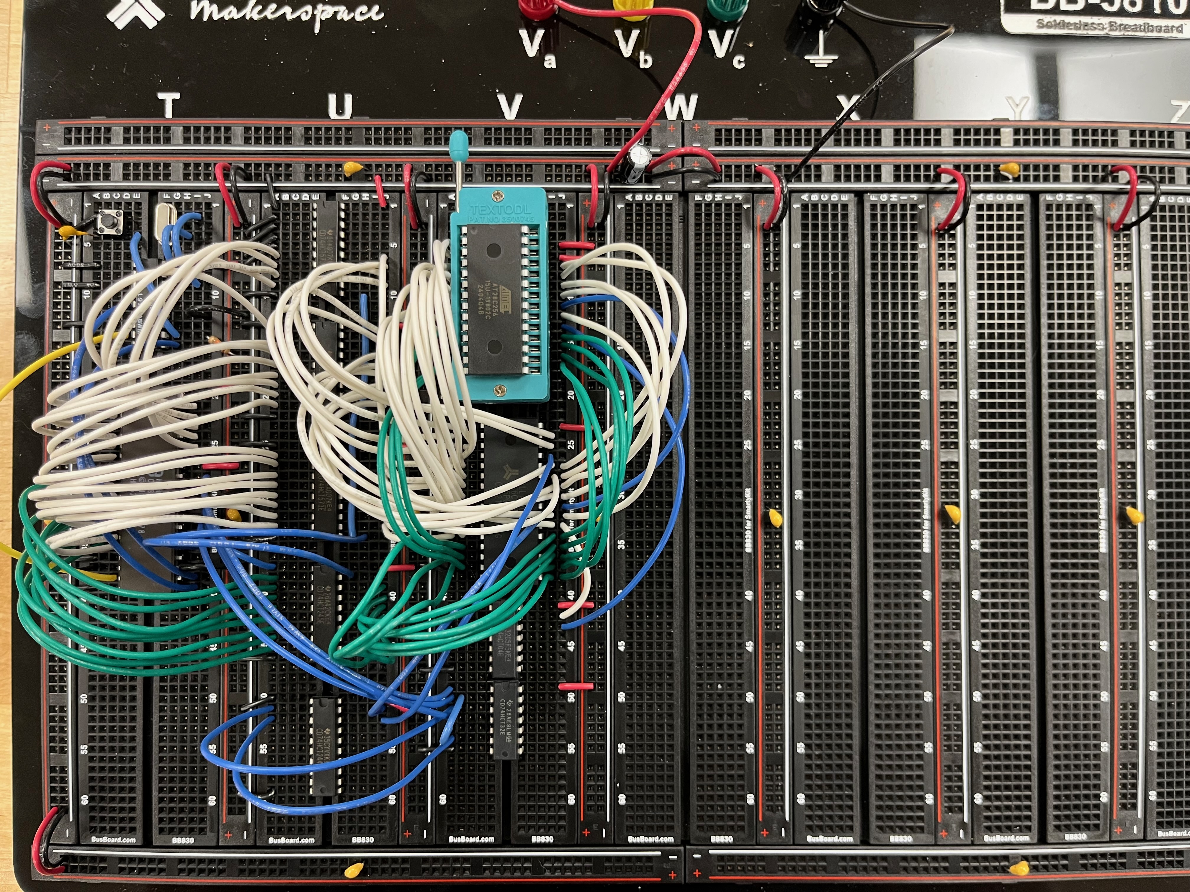
Your board should look similar to the following:
NOTE: This does not show the yellow clock signal wire. The 74HCT245 is still missing a GND wire in this image.
Lab Report
Take a picture of your breadboard. On this image or on a sketch with the 74HCT573 and 74HCT245 chips oriented appropriately, label Address bits 0-19 and Data bits 0-7.
Step 4: Wire up Memory#
Finally, our processor needs some memory to store instructions and data. We will use a 32KB ROM to store the firmware of the computer and a 512KB SRAM for read/write memory. We will wire both up to the processor, but we really only need the ROM for this lab.
The ROM is located at addresses 0xF8000 to 0xFFFFF, and the SRAM is located at addresses 0x00000 to 0x7FFFF. Note the gap in addresses. To simplify decoding the address to select the correct memory chip, we will enable the ROM when the address is in the range 0x80000 and above (using a single inverter). This is a bit of a hack, but should be sufficient for this computer.
We will be wiring up the schematic shown below.

Connect ICs and Power#
Connect the following power wires:
XS black: V-18-A — GND
XS black: V-38-A — GND
XS red: V-23-J — VCC
XS red: V-6-J — VCC
XS red: V-5-J — VCC
Insert the ZIF adapter (green box with pins) with pin 1 (near the arm) at V-5-E
Make sure the ZIF arm is pointing straight up and the slots are open
Insert the AT28C256 ROM (U11) into the ZIF socket with pin 1 near the arm
Close the ZIF arm to clamp down on the ROM
Insert the 6C4008 SRAM (U12) with pin 1 at V-23-D
Warning
Someone who did not wire the breadboard should now verify the above steps were completed correctly.
Your board should look similar to the following:
NOTE: This shows the ZIP arm closed. The arm should be lifted when inserting and removing the ROM.
Lab Report
Take a picture of your breadboard.
Connect Control, Address and Data#
Connect the following signal wires (blue):
M: U-52-J — V-31-I
M: U-53-J — V-26-I
M: V-31-J — V-11-J
M: V-43-J — V-13-J
Connect the following address wires (white):
S: U-26-J — V-27-A
S: U-27-J — V-28-A
S: U-28-J — V-29-A
S: U-29-J — V-30-A
S: U-30-J — V-31-A
S: U-31-J — V-32-A
S: U-32-J — V-33-A
S: U-33-J — V-34-A
S: V-34-J — V-42-J
M: U-6-J — V-33-I
M: U-7-J — V-23-A
M: U-8-J — V-25-I
M: U-9-J — V-24-A
M: U-14-J — V-24-I
M: U-15-J — V-25-A
M: U-16-J — V-27-I
M: U-17-J — V-26-A
M: U-18-J — V-30-I
M: U-19-J — V-32-I
M: U-20-J — V-29-I
M: U-21-J — V-28-I
M: V-5-A — V-25-B
M: V-6-A — V-26-B
M: V-7-A — V-27-B
M: V-8-A — V-28-B
M: V-9-A — V-29-B
M: V-10-A — V-30-B
M: V-11-A — V-31-B
M: V-12-A — V-32-B
M: V-13-A — V-33-B
M: V-14-A — V-34-B
M: V-7-J — V-28-J
M: V-8-J — V-27-J
M: V-9-J — V-29-J
M: V-10-J — V-30-J
M: V-12-J — V-32-J
Warning
Someone who did not wire the breadboard should now verify the above steps were completed correctly.
Connect the following data wires (green):
M: V-15-A — V-35-B
M: V-16-A — V-36-B
M: V-17-A — V-37-B
M: V-14-J — V-34-J
M: V-15-J — V-35-J
M: V-16-J — V-36-J
M: V-17-J — V-37-J
M: V-18-J — V-38-J
M: U-39-J — V-34-J
M: U-40-J — V-35-J
M: U-41-J — V-36-J
M: U-42-J — V-37-J
M: U-43-J — V-38-J
M: U-44-J — V-37-A
M: U-45-J — V-36-A
M: U-46-J — V-35-A
Warning
Someone who did not wire the breadboard should now verify the above steps were completed correctly.
At this point, your breadboard should be fully wired up. It should look similar to the following:
NOTE: The 74HCT245 is still missing a GND wire in this image. Two of the signal wires are also offset by one row in this image. Ensure you don’t make this mistake, too!
Lab Report
Take a picture of your breadboard.
Test Your Computer#
Take your breadboard back to the oscilloscope station
Plug in the VCC and GND supply wires
Connect the probes as follows
Yellow: T-14-A
Light Blue: U-10-G
Magenta: T-15-H
Dark Blue: U-52-G
Connect the grounds from the probes to ground
Make sure the RUN/STOP button is green on the scope. Press it until it lights up green
Press ON/OFF on the power supply
You should now see four signals recorded, similar to the following:
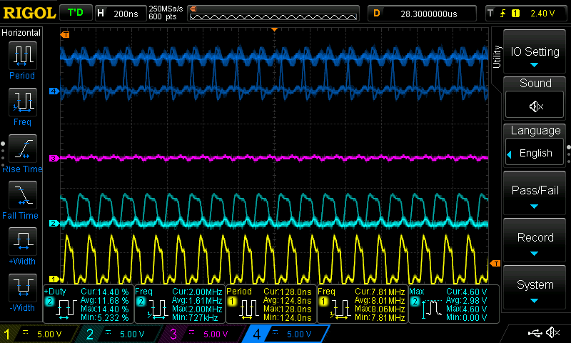
Congratulations, your computer is now running! In theory, these signals should run forever since the computer is running an infinite loop.
If you do not see these signals, you may have a wiring error. Press the ON/OFF button, disconnect the probes and power supply, and go back to your station to check your wiring.
Lab Report
Take a picture of the oscilloscope screen showing the memory signals. Label them with their meaning and describe what each signal does.
Try pressing the reset button on the breadboard a few times. You should see the signals change on the scope.
Lab Report
Describe the behavior of the signals when you press the reset button.
Press ON/OFF on the power supply
Disconnect all wires and return to your station
Step 5: Lab Cleanup#
Before you leave, make sure to clean up your station. This includes:
Placing all leftover components back in the foam or in the bags
Coiling up the power wires and placing them by the power supply
Turning off the power supply
Leaving your station neat and tidy
Step 6: Lab Report#
Collect your notes into a well formatted report that details your progress through this lab assignment. Begin the report with a brief abstract that describes the purpose of this lab (in your own words) and what you were able to achieve.
In the remainder of the report, be sure to address the callouts throughout this lab description. When screenshots or images are requested, provide a brief caption describing what is being shown.
Finally, discuss the program that actually run on the computer. You can see the assembly program used to generate the contents of ROM here.
What does this code do? Why do we pad up to 0xFFFF0? How does this map to the C program shown at the beginning of this lab?
Include this discussion of software in your lab report.