Lab 03: Breadboard Computer Part 2#
In this lab, we will modify our computer to add output. Then we will write and run a program to display a message on the output device.
Preliminaries#
Wires#
You are provided with a variety of wires to connect components together. There should be enough to complete this lab, but you may need to request additional wires. There are four different lengths of wires used in this computer:
Extra Small (XS), which can connect holes at most three apart
Small (S), which can connect holes at most twelve apart
Medium (M), which can connect holes at most 45 apart
Long (L), which can connect holes at most 70 apart
There are six different colors of wires, which we use to indicate the kind of signal being carried:
Red: Power +5V (VCC) and Interrupts
Black: Ground (GND)
Blue: Control Signals
White: Address Signals
Green: Data Signals
Yellow: Clock Signals
Prepare for the lab#
Make sure that you have all the items needed for this lab:
Computer from Lab 02
Electrostatic foam with chips and passive components
22 AWG hookup wire of lengths XS, S, and M
Bench Power Supply
2 Banana Wires
Tweezers
Chip Puller
USB Flash Drive
You may wish to organize the wires by length and color to make them easier to find. Keeping things organized and tidy will help you work more efficiently.
The components on the electrostatic foam are organized so that you can easily find each item. You can reference the part number on the foam to the schematic diagrams in this lab to find the correct component. The component ID (unique for each element) is shown on the diagram of the foam below:

There will be a significant amount of reading to follow along with this lab. Details matter, so take your time and make sure you understand each step before moving on. If you have any questions, don’t hesitate to ask!
Within your group, make sure that everyone is participating. If one person is wiring up the computer, another could be reading off the steps and marking them as complete. A third person can then verify that wires have been connected correctly. Mistakes are bound to happen, and this will help you track everything.
Step 1: Fix Bugs from Lab 02#
There are a few things we need to fix from Lab 02 before we can move on. Some of these changes are to give more space for wires, while others fix the computer’s operation (which would arbitrarily halt).
Connect the following wires:
XS red: T-10-A — VCC
XS red: T-12-A — VCC
Move the green address wires connected in U-38-A through U-45-A into the B column (one hole to the right)
Move the green address wires connected in U-39-J through U-46-J into the I column (one hole to the left)
Move the following blue control signal wires:
U-52-A to U-53-A
U-53-J to U-54-J
Move the following address wire:
V-7-J to V-7-I
Warning
Someone who did not wire the breadboard should now verify the above steps were completed correctly.
Your updated computer should look like the following:
Lab Report
Take a picture of your breadboard.
Test Your Computer#
Let’s verify that everything is working correctly before moving on. We will repeat the oscilloscope test from the end of Lab 02.
Take your breadboard to the oscilloscope station
Plug in the VCC and GND supply wires
Connect the probes as follows
Yellow: T-14-A
Light Blue: U-10-G
Magenta: T-15-H
Dark Blue: U-52-G
Connect the grounds from the probes to ground
Make sure the RUN/STOP button is green on the scope. Press it until it lights up green
Press ON/OFF on the power supply
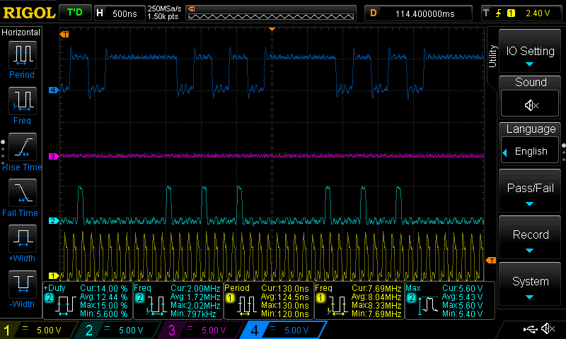
You should now see four signals recorded, similar to the following:
Lab Report
Take a picture of the oscilloscope screen showing the memory signals. Label them with their meaning and describe what each signal does.
Press the ON/OFF button on the power supply to turn off the computer
Disconnect the oscilloscope probes
Next, we will test that all the address wires are connected correctly to the ROM. We will use a logic analyzer to measure the digital signals on each address pin of the ROM chip to verify that the computer is counting correctly.
Carefully bend the address wires away from the ZIF socket on the ROM chip. Be sure no wires get unplugged!
Remove your ROM chip from the ZIF socket
Insert the ROM chip connected to the logic analyzer. It will have many wires connected to it.
Plug the white jumper wires in to GND
Plug the black jumper wire into U-10-G
Plug the purple jumper wire into T-14-A
In the DSView software, click
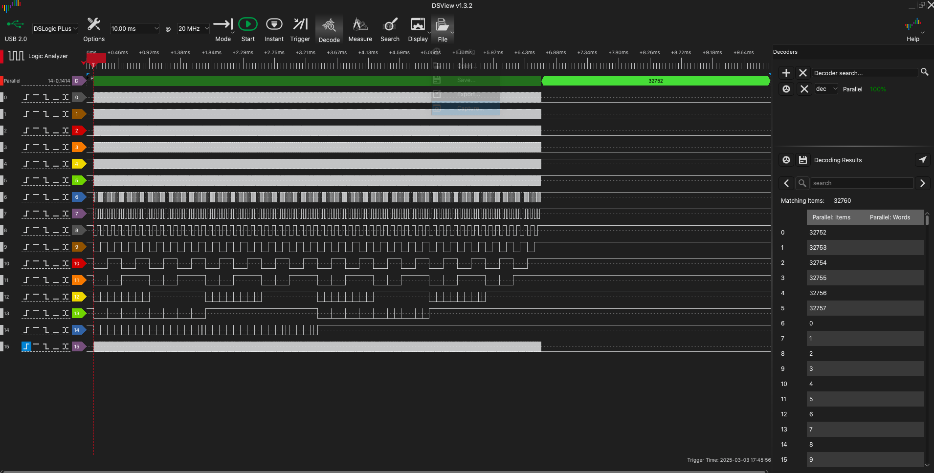
Run. It will indicate that the software is waiting for a trigger.Press the ON/OFF button on the power supply. The software should now show a graph of the address lines counting up and down.
It should look similar to the following:
Lab Report
Save a copy of the logic analyzer output to your flash drive. Include it in your lab report.
Export the data to a CSV file. Compare it with the expected values in the table below. If they don’t match, verify all of your wires from the latches to the memory chips and try again.
Address
32752
32753
32754
32755
32756
32757
0
1
2
…
32752
32752
You can write a simple python program to generate this list of numbers and then use a compare tool (e.g., Visual Studio Code or DiffChecker) to compare the two files. Note that the last number is repeated twice. This is because the computer latches the address one final time as it is halting.
Congratulations, you have a computer with a CPU and memory that is tested to be working correctly!
Step 2: Add an LCD Output#
Next, we will add an LCD display to your computer to display output. This will
be our fist IO device. IO devices in x86 use a separate IO address space. That
is, there are separate addresses to communicate with the IO devices, which are called ports. Port 0x3F8 is different from memory address 0x3F8. In x86, ports are accessed using special in and out instructions.
Lab Report
Look up how big the IO address space is for the 8088 CPU. Report on how this compares with the memory address space.
We will need separate IO Read and Write control lines (currently your computer only decodes Memory Read and Write). Further, we need to choose which IO device is being accessed base on the address or port used by the CPU. We will use a demultiplexer or decoder to generate enable signals for a variety of IO devices based on the address provided. This device takes a number of address lines and generates a signal for one of \(N\) output lines based on the address. We will use a 74HCT138, which has 3 address lines and 8 output lines.
The schematic of our computer after this step is shown below:

Connect ICs and Power#
Insert the 74HCT138 demultiplexer (U14) with pin 1 at W-4-E
Insert the 82C55A PIO (U16) with pin 1 at W-15-C
PIO stands for programmable input/output. Some documentation may refer to this as a PPI, or programmable peripheral interface.
This is an interface chip that the CPU can write and read from. It can control 24 pins to set them high or low (or read if another chip is driving the pin high or low).
We will use this chip to control the LCD display, which expects specific bit patterns and control signals to display characters. By programmatically generating these signals, we are bit-banging the LCD.
Move the ceramic capacitor in the power rails between X and Y down to about rows 40-41
Insert the LCD module with pin 1 in X-35-C and pin 16 in X-20-C
Insert the variable resistor R5 with pin 1 in X-2-D, pin 2 in X-3-C, and pin 3 in X-4-D (pins 1 and 3 are labelled on the top of the resistor)
Insert the variable resistor R6 with pin 1 in X-2-G, pin 2 in X-3-F, and pin 3 in X-4-G (pins 1 and 3 are labelled on the top of the resistor)
Turn both resistor knobs until they point down at the LCD module
Connect the following wires:
XS black: W-7-A — GND
XS black: W-11-A — GND
XS black: W-21-A — GND
XS black: X-35-A — GND
XS black: X-4-A — GND
S back: X-4-J — GND
M back: X-20-A — X-3-J
XS red: W-29-J — VCC
XS red: W-4-J — VCC
S red: W-9-A — VCC
S red: X-34-A — VCC
S red: X-21-A — VCC
S red: X-2-A — VCC
S red: X-2-J — VCC
M red: X-33-A — X-3-A
Warning
Someone who did not wire the breadboard should now verify the above steps were completed correctly.
Lab Report
Take a picture of your breadboard.
Connect Control, Address, and Data#
Connect the following signal wires (blue):
S: V-46-D — V-50-G
S: V-49-D — V-51-G
S: V-52-D — V-53-G
S: V-45-A — V-50-C
S: V-50-H — V-54-H
M: U-55-A — V-51-G
M: U-57-A — V-55-G
M: V-50-J — W-8-A
M: U-56-J — W-48-H
M: U-58-J — W-47-H
M: W-48-I — W-19-B
M: W-47-I — W-19-H
M: T-40-J — V-46-G
M: V-46-J — W-20-H
M: W-20-B — W-7-G
Warning
Someone who did not wire the breadboard should now verify the above steps were completed correctly.
Connect the following address wires (white):
S: V-7-J — W-4-A
M: V-5-B — W-5-A
M: V-24-J — W-6-A
M: U-33-I — W-22-A
M: U-34-I — W-23-A
Connect the following data wires (green):
M: U-39-J — W-37-A
M: U-40-J — W-38-A
M: U-41-J — W-39-A
M: U-42-J — W-40-A
M: U-43-J — W-41-A
M: U-44-J — W-42-A
M: U-45-J — W-43-A
M: U-46-J — W-44-A
M: U-37-E — W-28-H
M: U-38-E — W-27-H
M: U-39-E — W-26-H
M: U-40-E — W-25-H
M: U-41-E — W-24-H
M: U-42-E — W-23-H
M: U-43-E — W-22-H
M: U-44-E — W-21-H
Warning
Someone who did not wire the breadboard should now verify the above steps were completed correctly.
Wire the following signal wires (blue):
S: W-30-H — X-22-A
HINT: pre-bend the ends of these short wires to fit
S: W-31-H — X-23-A
S: W-32-H — X-24-A
S: W-33-H — X-25-A
S: W-34-H — X-26-A
M: W-34-A — X-27-A
M: W-33-A — X-28-A
M: W-32-A — X-29-A
M: W-30-A — X-32-A
M: W-29-A — X-31-A
M: W-28-A — X-30-A
Warning
Someone who did not wire the breadboard should now verify the above steps were completed correctly.
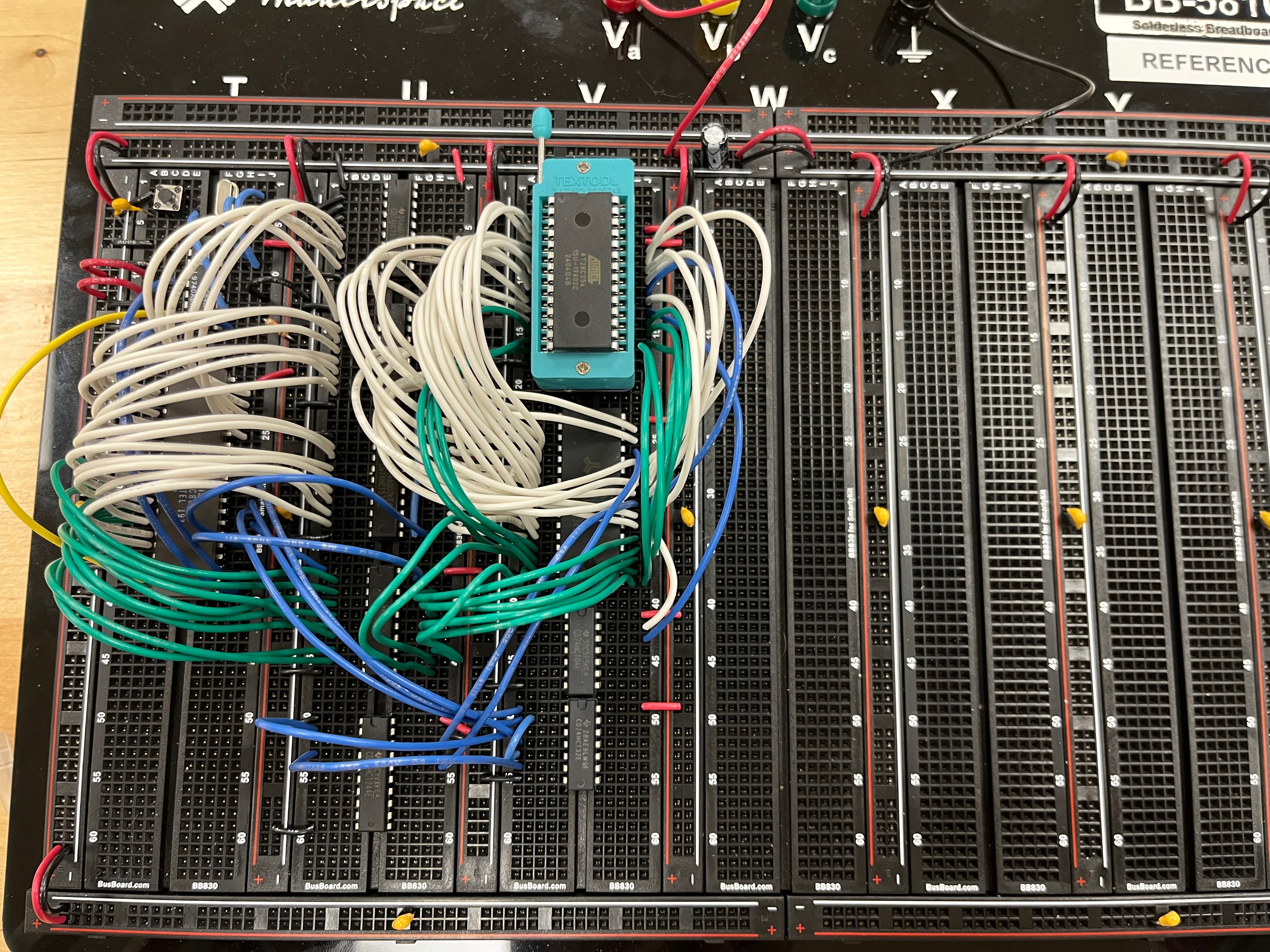
Your completed computer should look similar to:
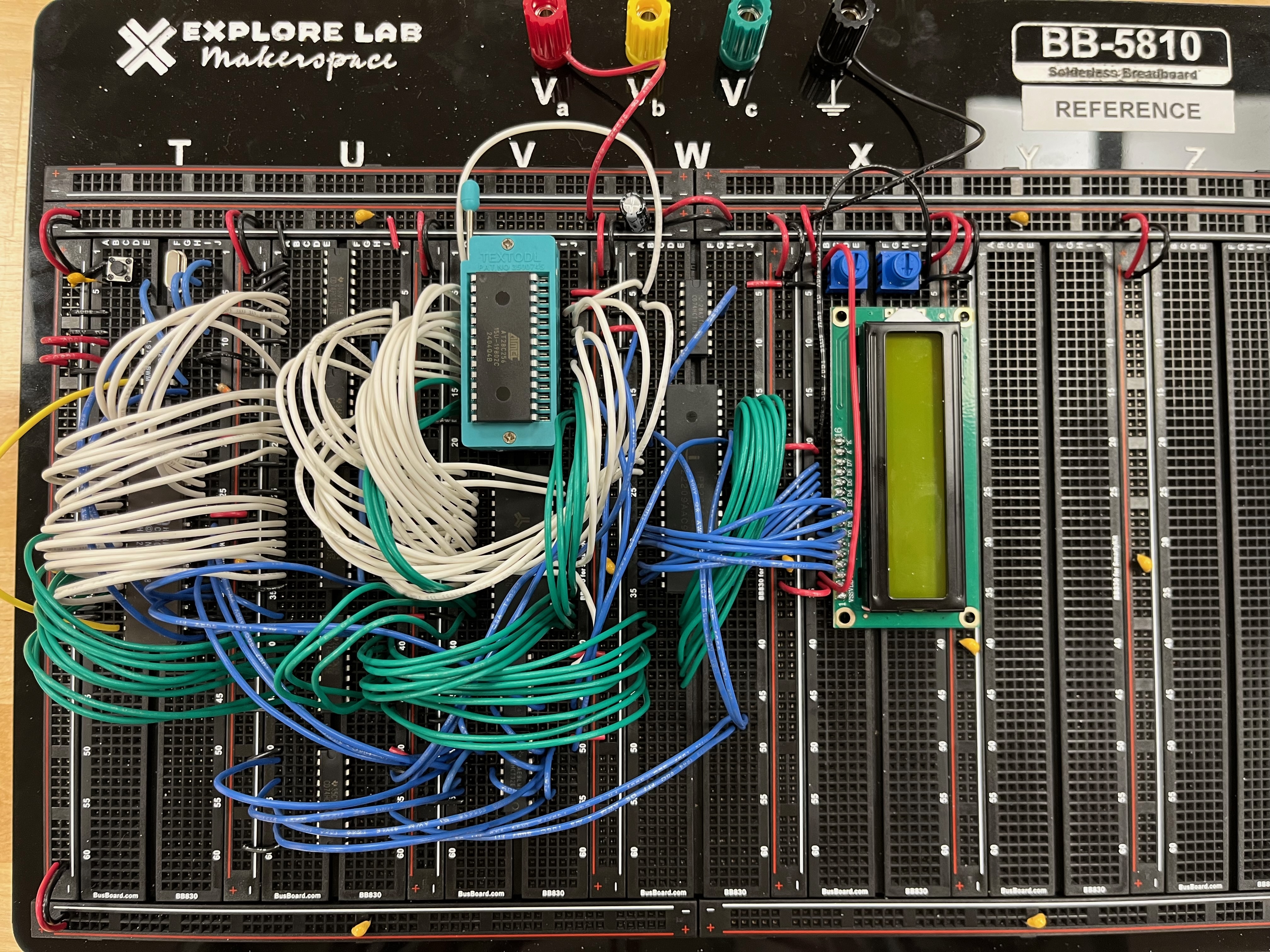
Lab Report
Take a picture of your breadboard.
Step 3: Program the ROM#
Test the LCD#
Now, we have to write a program to display a message on the LCD. Before doing this, let’s test that the LCD is working correctly.
Download a copy of
hello.binto your flash driveNote
Copies of the infinite loop and address test ROMs are also available.
Remove the ROM chip from your computer by lifting the bar on the ZIF socket and removing the chip
Take your flash drive and ROM chip to the computer with the ROM programmer.
Insert the ROM chip into the programmer and the flash drive into the computer
From a terminal, run the following command:
minipro -p AT28C256 -uP -w /path/to/hello.bin
Replace
/path/to/hello.binwith the path to the file on your flash drive, which you can do by dragging the file into the terminal window.Once the command completes, remove the ROM chip from the programmer
Eject your flash drive from the computer by dragging its icon to the trash
Insert the ROM chip back into the ZIF socket on your computer and lower the bar
Hook up power to your computer and turn it on with the ON/OFF button
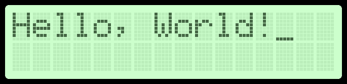
You should see the LCD display “Hello, World!”.
The left adjustable resistor (or potentiometer—pot) controls the contrast of the display. If you can’t see the text, adjust this knob.
The right pot controls the backlight brightness. If you can’t see the display, adjust this knob.
If you press the reset button, the message should reappear
If this program does not work, double-check all of your wiring from Step 2. You may wish to compare with the reference computer. Congratulations! You have successfully added an output device to your computer!
Lab Report
Take a picture of the LCD displaying “Hello, World!”.
Write Your Own Hello World#
Now that you have a working LCD, let’s write our own program to display a message on the screen. Use the same development environment we set up in Lab 1 to write and assemble your x86 program.
Download a copy of lcd_helper.asm to your computer VSCode project. This file contains the assembly instructions needed to set up the LCD display.
A few things to note:
The LCD data pins are connected to
PORTBof the PIO chipThe LCD control pins are connected to
PORTCof the PIO chipThe PIO chip has four control registers. Each is accessed from a unique IO port on the x86.
Three of the ports are used to read/write the pins on the chip, which are grouped into three 8-bit ports:
PORTA,PORTB, andPORTC:PORTA is located at 0x4000
PORTB is located at 0x4001
PORTC is located at 0x4002
The fourth port is used to control the chip itself (e.g., whether a PORT is in read or write mode):
CTRL is located at 0x4003
Set up a new assembly file (e.g., lab3.asm) to write out Hello World program. You can use the following template to get started:
; simple hello world kernel for the ASM86-512 computer
; by YOUR NAME
BITS 16

; the ROM is 32KiB, so the chip will start of 0xF8000...the highest 32KiB of the
; address space
ORG 0xF8000

; include the helper functions
%include "lcd_helper.asm"

;;;;;;;;;;;;;;;;;;;;;;;;;;;;;;;;;;;;;;;;;;;;;;;;;;;;;;;;;;;;;;;;;;;;;;;;;;;;;;;;
; Print Hello World Message                                                    ;
;;;;;;;;;;;;;;;;;;;;;;;;;;;;;;;;;;;;;;;;;;;;;;;;;;;;;;;;;;;;;;;;;;;;;;;;;;;;;;;;

  ; set the DS to the ROM address space
  ; this is useful if you want to use the lodsb instruction
  xor ax, ax
  or ax, 0xF000
  mov ds, ax

; TODO insert your code here

; at the end of your program, add a halt instruction to stop the CPU
; we'll follow this by a jump back to halt just to be safe
halt:
  hlt
  jmp halt

; TODO put any data here

; pad up to 0xFFFF0 (the location of the reset vector)
  times (0xFFFF0 - 0xF8000) - ($ - $$) db 0

  ; this is the code that will be run on power-up
  ; we will do a long jump (a jump with a segment) to the start of our ROM
  jmp 0xF000:0x8000

  ; pad to 0xFFFFF (the end of the address space)
  ; $ represents the current address, and $$ represents the starting address
  times (0x100000 - 0xF8000) - ($ - $$) db 0
Fill in the TODO sections with your code. Note that we are running with ROM
only. That means you can use the stack or any call, push, or pop
instructions.
Interfacing with the LCD#
To communicate with the LCD, you will need to:
Load the byte of data you wish to send to the LCD into
alLoad the control register into
dxIssue the
out dx, axinstruction to send the data inalto the port stored indx
Full documentation on the LCD commands can be found in the HD44780 datasheet; however, we will describe the basics here.
To write a character to the LCD, you will need to:
Output the ASCII character to the
PORTBregisterSet the RS bit to 1 (indicating that you are writing data)
Send a pulse to the E bit (indicating that you are sending data)
Set the RS bit back to 0
Wait for the LCD to process the data
        gantt
  title LCD Data Write Timing
  dateFormat  HH:mm:ss
  axisFormat  %H:%M:%S
  section LCD Write
  E Bit Pulsed               :done, 00:00:04, 00:00:06
  RS Bit Set to 1            :done, 00:00:02, 00:00:08
  ASCII Data Valid on PORT B :done, 00:00:00, 00:00:10
Checking to see if the LCD has processed the instruction to write the character is a bit more complicated. The LCD has a busy flag that is set when it is processing an instruction. To check if the LCD is busy, you will need to:
Switch
PORTBto input modeSet the RW bit to 1 (indicating that you are reading data)
Send a pulse to the E bit (indicating that you are sending data)
Read the data from the
PORTBregisterCheck if bit position 7 is set to 1
If the bit is 1, the device is busy and we need to wait
If the bit is 0, the device is ready to accept more data
Set the RW bit back to 0
Set
PORTBback to output mode
To write A to the LCD, the basic process looks like:
  ; write the character `A` to the LCD
  mov al, 'A'
  mov dx, PORTB
  out dx, al
  ; set RS bit to send data
  mov al, RS
  mov dx, PORTC
  out dx, al
  ; set E bit to send data
  mov al, RS | E
  out dx, al
  ; clear E bit
  mov al, RS
  out dx, al
  ; clear RS/RW/E bits
  mov al, 0
  out dx, al

  ; wait for the LCD to process the instruction
  ; set PORT B to input
  mov al, 0b10000010
  mov dx, CTRL
  out dx, al
p1:
  ; toggle the RW pin
  mov al, RW
  mov dx, PORTC
  out dx, al
  ; set E bit to send instruction
  mov al, E | RW
  out dx, al
  ; read the busy flag
  mov dx, PORTB
  in al, dx
  and al, 0x80
  ; if the busy flag is set, try again
  jne p1
  ; clear the E and RW pins
  mov al, 0
  mov dx, PORTC
  out dx, al
  ; set PORT B back to output
  mov al, 0b10000000
  mov dx, CTRL
  out dx, al

  ; output 0s to PORT B
  mov al, 0
  mov dx, PORTB
  out dx, al

  ; output 0s to PORT C
  mov al, 0
  mov dx, PORTC
  out dx, al
Adapt this code into your program to display your message on the LCD. You should only need to change the first line. This code will like be the body of a loop.
Testing Your Program#
Danger
Ensure that your computer is powered off (the green power light on the supply is off) before inserting or removing the ROM chip!
Assemble your program using nasm:
nasm -f bin lab3.asm -o lab3.bin
Copy the
lab3.binfile to your flash drive. Remove the ROM chip from your computer and program it with your ROM binary:minipro -p AT28C256 -uP -w /path/to/lab3.bin
Insert the ROM chip back into your computer and power it on
You should see your message displayed on the LCD
Lab Report
Film a video of your computer displaying your message on the LCD. Include the video in your lab report upload.
Step 4: Lab Cleanup#
Before you leave, make sure to clean up your station. This includes:
Placing all leftover components back in the foam or in the bags
Coiling up the power wires and placing them by the power supply
Turning off the power supply
Leaving your station neat and tidy
Step 5: Lab Report#
Collect your notes into a well formatted report that details your progress through this lab assignment. Begin the report with a brief abstract that describes the purpose of this lab (in your own words) and what you were able to achieve.
In the remainder of the report, be sure to address the callouts throughout this lab description. When screenshots or images are requested, provide a brief caption describing what is being shown.
Make sure to also submit a copy of your final program that displays your message on the LCD as well as a video of your computer running.