Lab 04: Breadboard Computer Part 3#
In this lab, we will modify our computer to add a number of I/O devices necessary for booting and running a simple operating system. We will add a programmable interrupt controller, a programmable timer, a serial port controller, a CompactFlash interface, and a speaker. Taken together, these devices will allow us to perform a Power-On Self Test (POST) and execute a bootloader from disk.
The schematic of our computer after this lab is shown below:

A PDF version of the schematic is available here.
Preliminaries#
Wires#
You are provided with a variety of wires to connect components together. There should be enough to complete this lab, but you may need to request additional wires. There are four different lengths of wires used in this computer:
Extra Small (XS), which can connect holes at most three apart
Small (S), which can connect holes at most twelve apart
Medium (M), which can connect holes at most 45 apart
Long (L), which can connect holes at most 70 apart
There are six different colors of wires, which we use to indicate the kind of signal being carried:
Red: Power +5V (VCC) and Interrupts
Black: Ground (GND)
Blue: Control Signals
White: Address Signals
Green: Data Signals
Yellow: Clock Signals
Prepare for the lab#
Make sure that you have all the items needed for this lab:
Computer from Lab 03
Electrostatic foam with chips and passive components
IDE/PATA connector to breadboard adapter
CompactFlash to IDE/PATA adapter
USB to Serial adapter
Speaker
22 AWG hookup wire of lengths XS, S, M, and L
Bench Power Supply
2 Banana Wires
Tweezers
Chip Puller
USB Flash Drive
CompactFlash Card
USB Cable
You may wish to organize the wires by length and color to make them easier to find. Keeping things organized and tidy will help you work more efficiently.
The components on the electrostatic foam are organized so that you can easily find each item. You can reference the part number on the foam to the schematic diagrams in this lab to find the correct component. The component ID (unique for each element) is shown on the diagram of the foam below:

Note
Many of these components are already placed on the breadboard. All components are shown in their original positions.
As with past labs, there will be a significant amount of reading to follow along with this lab. Details matter, so take your time and make sure you understand each step before moving on. If you have any questions, don’t hesitate to ask!
Within your group, make sure that everyone is participating. If one person is wiring up the computer, another could be reading off the steps and marking them as complete. A third person can then verify that wires have been connected correctly. Mistakes are bound to happen, and this will help you track everything.
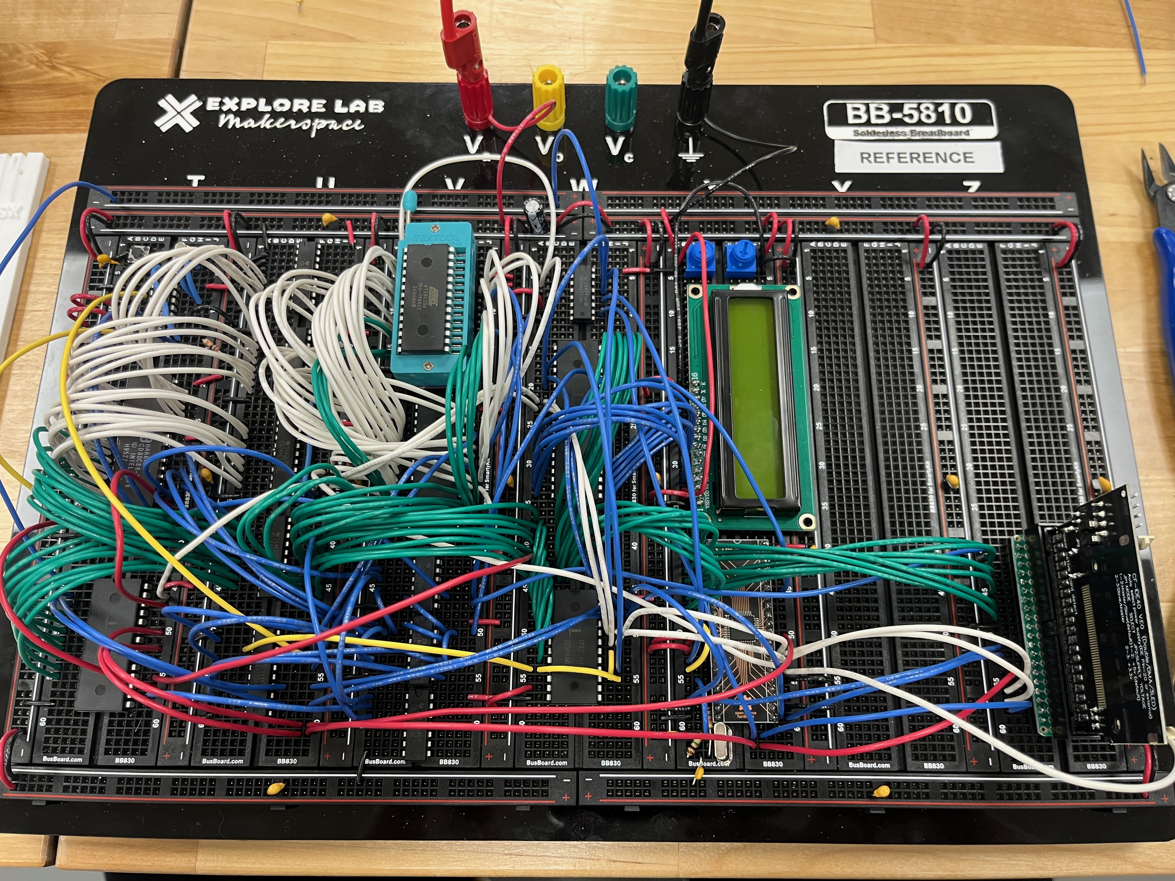
Step 1: Wire Up the Programmable Interrupt Controller#
The interrupt controller is used to manage a number of interrupts from the I/O devices. Since the 80C88 processor only has one interrupt pin, this device is used to prioritize and manage multiple interrupts.
Insert the 8259A controller (U13) with pin 1 at T-45-D
Insert the 74HCT00 NAND gate (U9) with pin 1 at V-57-E
Remove the XS black wire from T-37-A to ground (we will wire a signal from the 8259A to this pin)
Wire up power and ground
XS Black: T-58-A — GND
XS Black: V-63-A — GND
XS Red: T-45-J — VCC
XS Red: V-57-J — VCC
Wire up the control signal wires (blue):
Unplug U-38-G and plug it into V-43-A
M: V-44-A — V-57-A
M: T-57-J — V-58-A
M: U-38-J — V-59-A
M: U-56-G — T-47-A
M: U-58-G — T-44-A
M: W-5-G — Top-Left-Power-Bus GND (note this is not actually ground)
L: Top-Left-Power-Bus GND — T-45-A
Wire up the data wires (green):
M: U-38-A — T-48-A
M: U-39-A — T-49-A
M: U-40-A — T-50-A
M: U-41-A — T-51-A
M: U-42-A — T-52-A
M: U-43-A — T-53-A
M: U-44-A — T-54-A
M: U-45-A — T-55-A
Wire up the address wires (white):
M: U-33-H — T-46-J
Wire up the interrupt wires (red):
M: T-37-C — T-56-J
M: T-36-J — T-47-J
Warning
Someone who did not wire the breadboard should now verify the above steps were completed correctly.
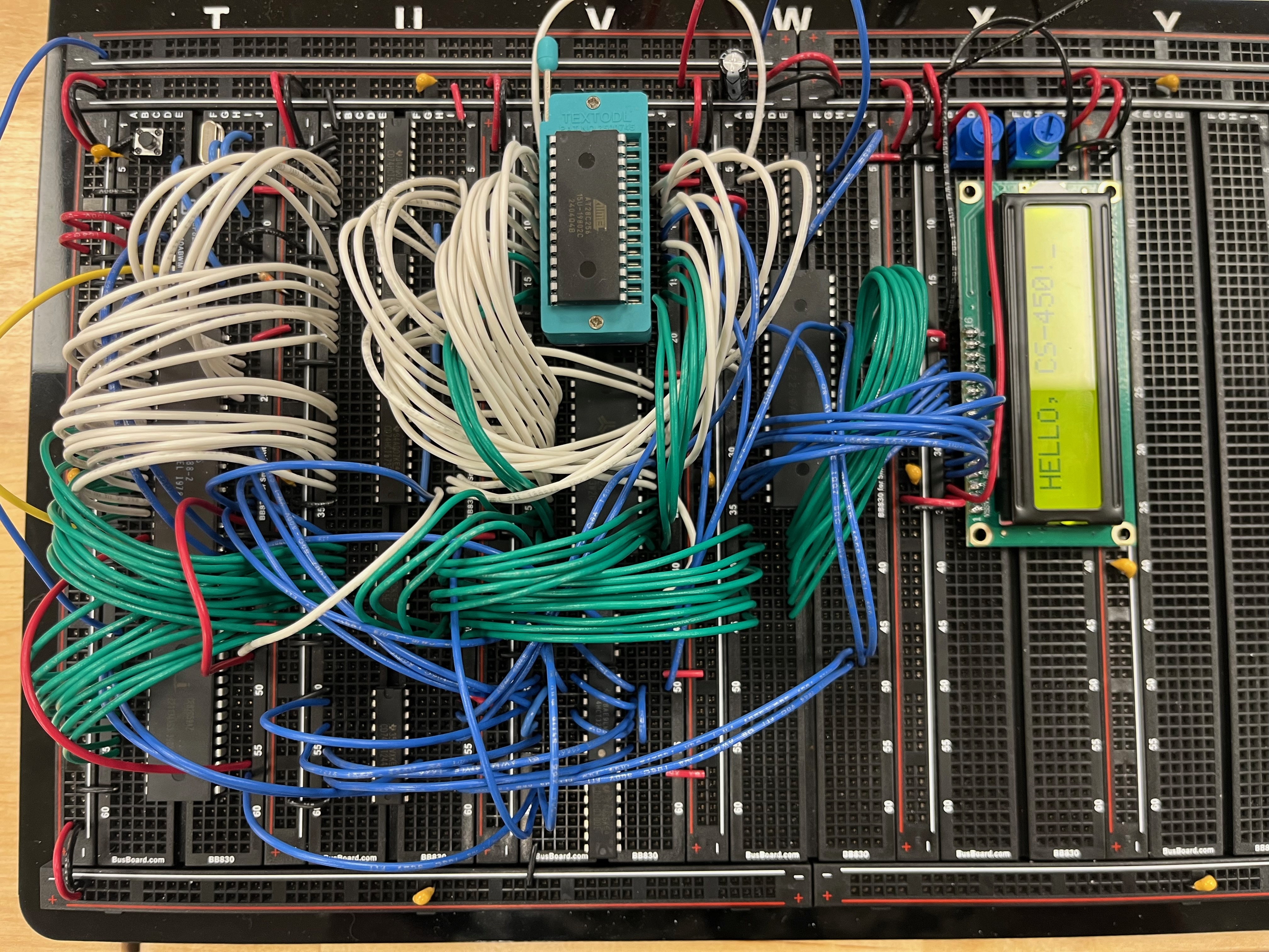
Your updated computer should look like the following:
Test your work#
Power on your computer and confirm that it still displays the greeting from the previous lab.
Lab Report
Take a picture of your breadboard.
Step 2: Wire up the Programmable Timer#
The programmable timer will be used to generate interrupts at regular intervals. This is useful for timing events in the operating system, such as scheduling. We also use it to generate a square wave signal for the speaker.
Insert the 8253 timer (U15) with pin 1 at W-46-C
Wire up power and ground
XS Black: W-57-A — GND
XS Red: W-46-J — VCC
S Red: W-56-A — VCC
Wire up the data wires (green):
S: W-37-B — W-46-B
S: W-38-B — W-47-B
S: W-39-B — W-48-B
S: W-40-B — W-49-B
S: W-41-B — W-50-B
S: W-42-B — W-51-B
S: W-43-B — W-52-B
S: W-44-B — W-53-B
HINT: pre-bend the wires slightly to make them easier to insert
Wire up the address wires (white):
M: W-22-B — W-50-H
M: W-23-B — W-51-H
Wire up the clock signal wires (yellow):
XS: W-52-H — W-55-H
S: W-54-B — W-55-I
M: U-52-D — W-54-A
L: T-8-D — U-53-J
Wire up the control signal wires (blue):
L: W-18-B — W-54-I
L: W-6-G — W-49-G
Wire up the interrupt signal wires (red):
L: T-55-J — W-55-A
Warning
Someone who did not wire the breadboard should now verify the above steps were completed correctly.
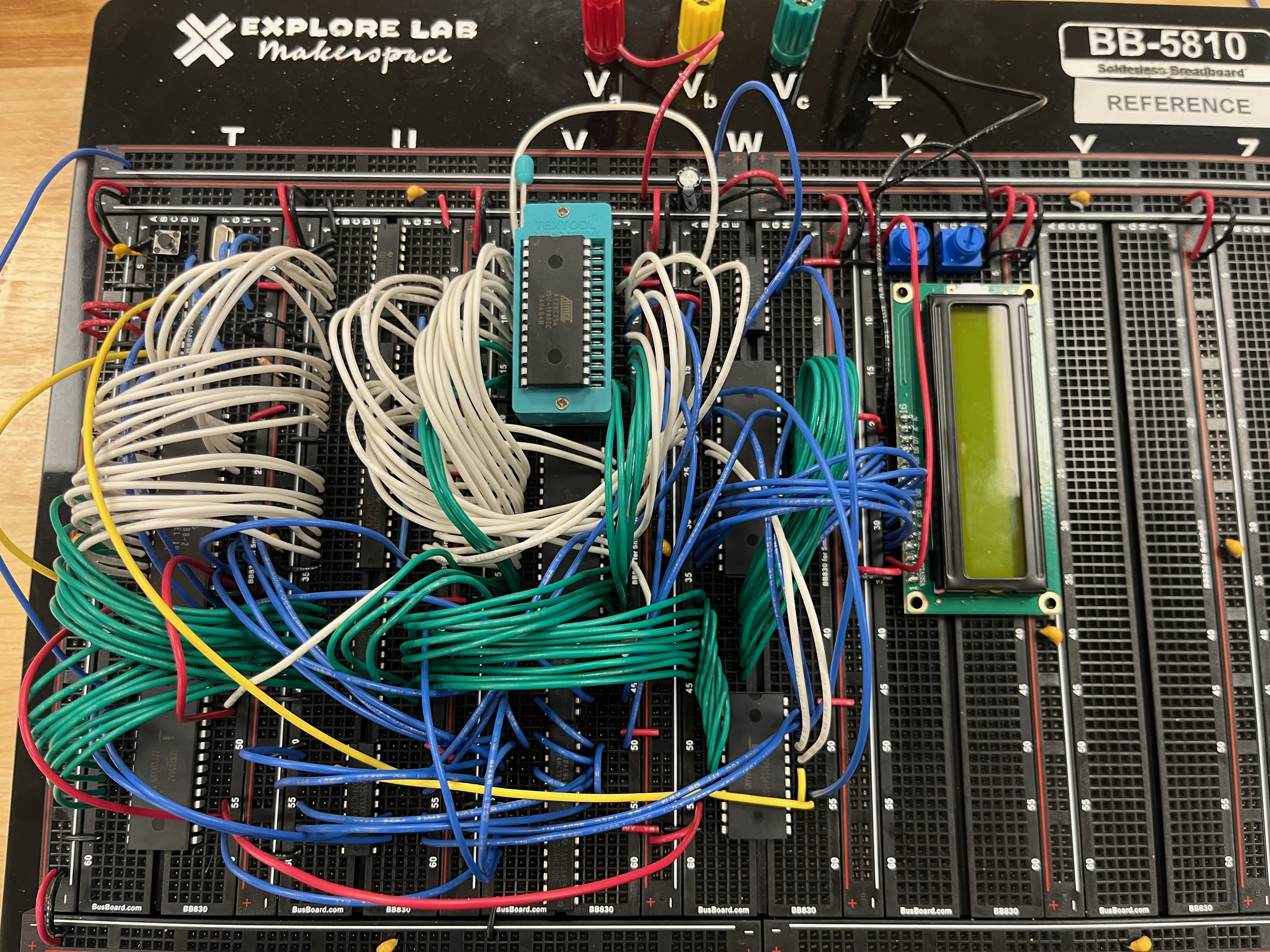
Your updated computer should look like the following:
Test your work#
Power on your computer and confirm that it still displays the greeting from the previous lab.
Lab Report
Take a picture of your breadboard.
Step 3: Wire up the Serial Port Controller#
The serial port will be our primary input/output device for the computer. It interfaces with our own computer using a serial to USB adapter and a terminal emulator program. Early computers would often interface with a terminal, a device with a screen and keyboard and very basic firmware. The terminal would communicate with the computer over a serial connection.
A serial controller often goes by other names such as UART (Universal Asynchronous Receiver Transmitter), COM port, or ACE (Asynchronous Communications Element).
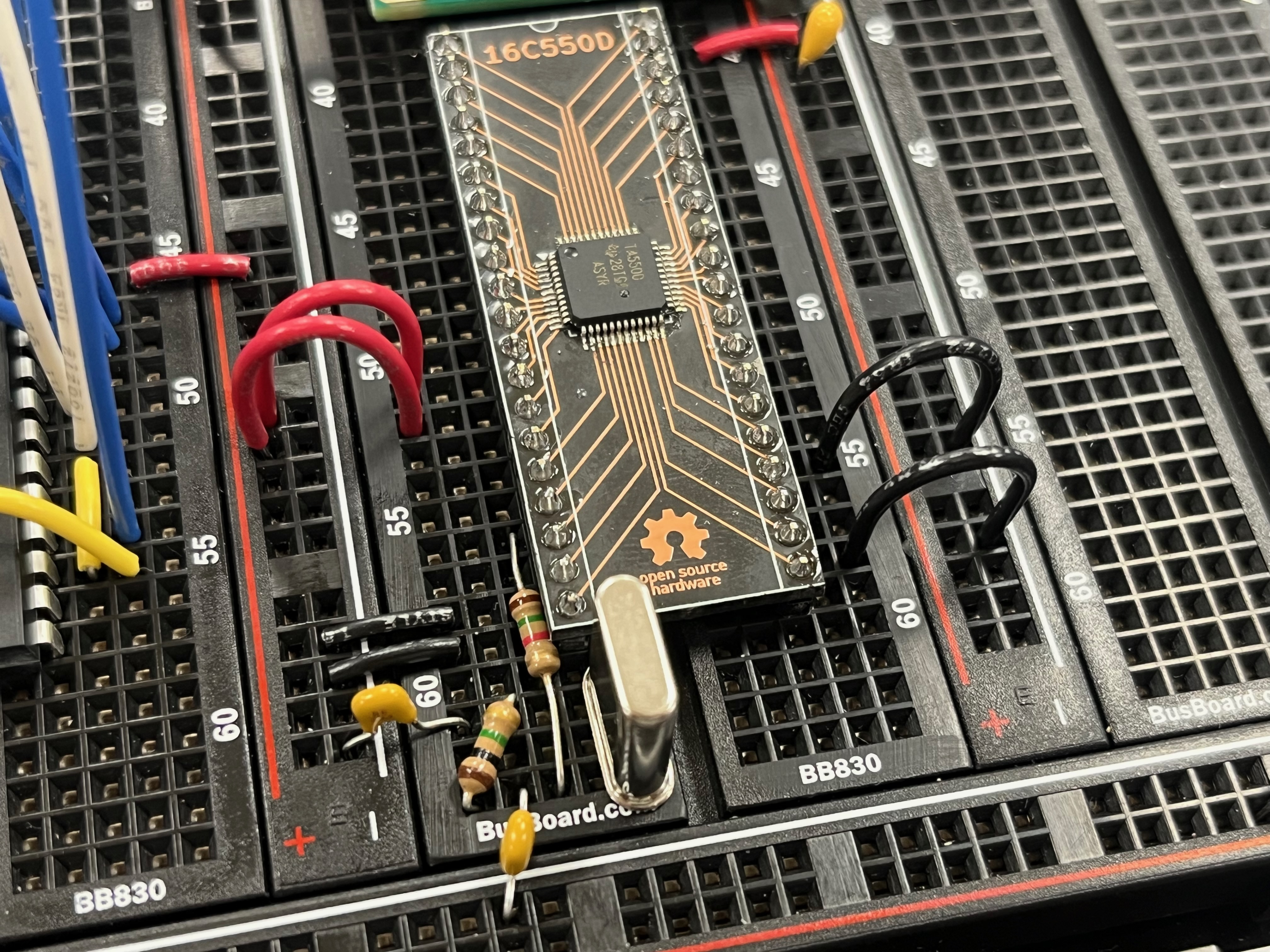
Insert the 16C550D UART (U18) with pin 1 at X-40-D
Insert the 3.072 MHz crystal (Y2) between X-61-E and X-63-E
Insert the Brown-Black-Green 1M resistor (R2) between X-61-B and X-63-A
HINT: pre-bend the wires together slightly to make them easier to insert
Insert the Brown-Green-Red 1.5M resistor (R3) between X-56-C and X-63-C
Insert the 22pF ceramic capacitor (C2) between X-61-A and GND
Insert the 47pF ceramic capacitor (C3) between X-63-B and GND
This is a tight fit. A close-up of the layout of these components is shown:
Wire up power and ground
XS Black: X-58-A — GND
XS Black: X-59-A — GND
S Black: X-58-J — GND
S Black: X-55-J — GND
XS Red: X-40-J — VCC
S Red: X-52-A — VCC
S Red: X-51-A — VCC
Wire up the clock signal wires (yellow):
S: X-48-A — X-54-A
Wire up the data wires (green):
Carefully shift the wires in W-37-E through W-44-E to the left into column D
M: W-37-E — X-47-A
M: W-38-E — X-46-A
M: W-39-E — X-45-A
M: W-40-E — X-44-A
M: W-41-E — X-43-A
M: W-42-E — X-42-A
M: W-43-E — X-41-A
M: W-44-E — X-40-A
HINT: The bit order on this chip is reversed from the others, so bus “twists” when you wire it up
Wire up the address wires (white):
M: W-50-J — X-53-I
M: W-51-J — X-52-I
L: U-31-I — X-54-I
HINT: Feed this wire from right to left under and through many of the data wires (see the reference)
Wire up the control signal wires (blue):
S: X-55-B — X-61-C
M: W-20-I — X-45-J
M: W-47-J — X-57-A
M: W-48-J — X-59-I
L: W-8-G — X-53-A
Wire up the interrupt signal wires (red):
M: T-52-J — U-60-I
L: U-60-J — X-50-J
Warning
Someone who did not wire the breadboard should now verify the above steps were completed correctly.
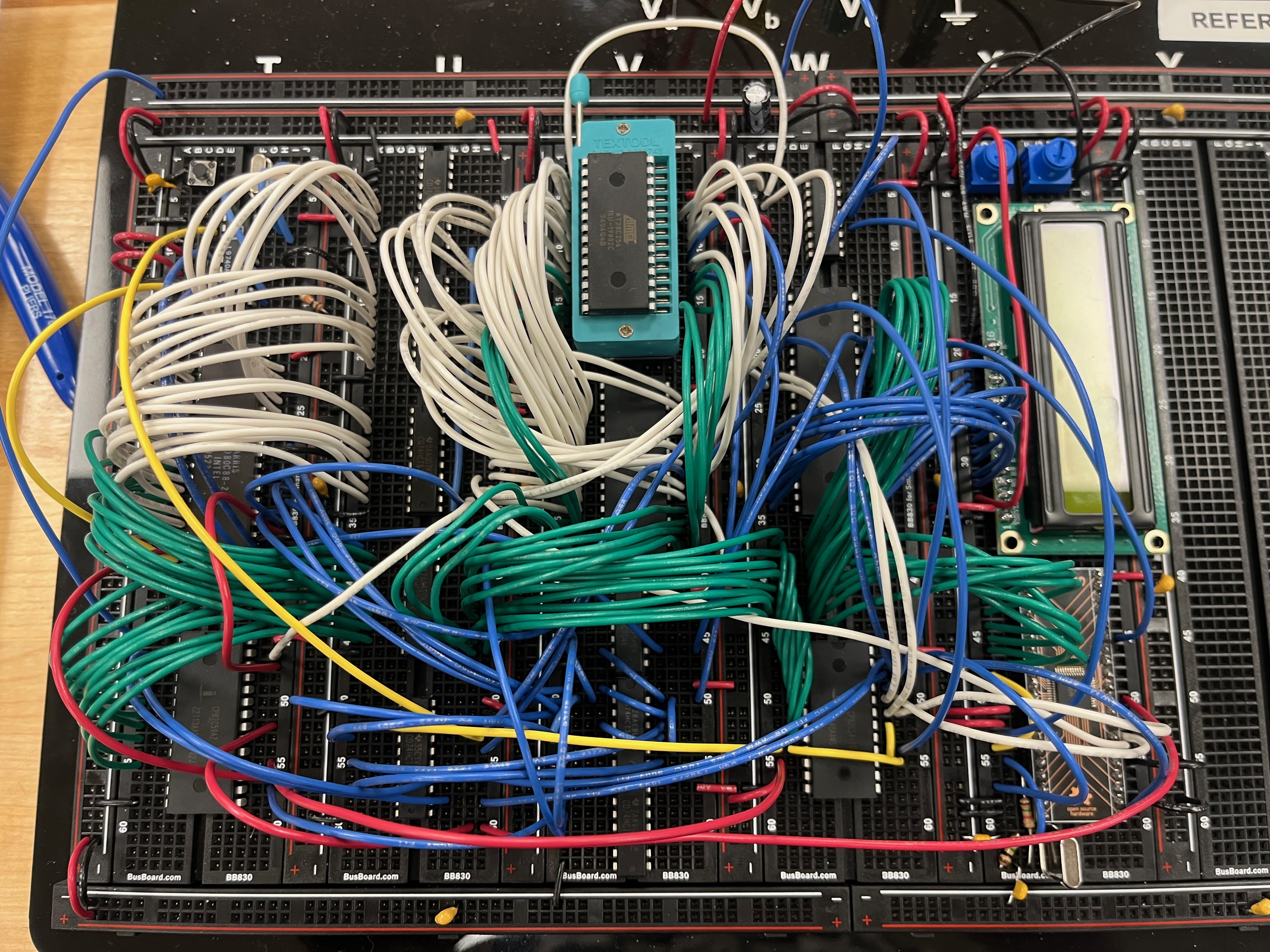
Your updated computer should look like the following:
Test your work#
Power on your computer and confirm that it still displays the greeting from the previous lab.
Lab Report
Take a picture of your breadboard.
Step 4: Wire up the CompactFlash Interface#
We will use a CompactFlash card as our primary storage device. This is a solid-state drive (SSD), but it uses the same IDE/PATA interface as older hard drives dating back to at least the IBM PC/AT. This interface turns out to be easy to interface directly with our processor and program at a low level!
Insert the PATA/IDE connector (J2) with pin 1 at Z-40-D
Note that pin 1 is on the side with the notch (i.e., the notch should face to the left)
Pin numbers on the IDE connector alternate sides (i.e., pin 1 is on the left, pin 2 is on the right, etc.)
Wire up power and ground
XS Black: Z-49-A — GND
XS Black: Z-59-J — GND
XS Red: Z-49-J — VCC
XS Red: Z-58-J — VCC
Wire up the control signal wires (blue):
M: X-57-B — Z-51-A
M: X-59-J — Z-52-A
M: X-61-G — Z-58-A
L: W-10-G — X-61-F
HINT: Feed this wire under the data wires
L: V-47-J — Z-40-A
Wire up the data wires (green):
M: X-47-B — Z-41-A
M: X-46-B — Z-42-A
M: X-45-B — Z-43-A
M: X-44-B — Z-44-A
M: X-43-B — Z-45-A
M: X-42-B — Z-46-A
M: X-41-B — Z-47-A
M: X-40-B — Z-48-A
HINT: The bus “twists” when you wire it up
Wire up the address wires (white):
M: X-52-J — Z-57-A
M: X-53-J — Z-56-A
L: X-54-J — Z-57-J
Wire up the interrupt signal wires (red):
M: T-50-J — U-61-I
L: U-61-J — X-62-F
M: X-62-G — Z-55-A
Insert the CompactFlash adapter into the IDE/PATA connector
Warning
Someone who did not wire the breadboard should now verify the above steps were completed correctly.
Your updated computer should look like the following:
Test your work#
Power on your computer and confirm that it still displays the greeting from the previous lab. The red power LED on the CF adapter should be lit.
Lab Report
Take a picture of your breadboard.
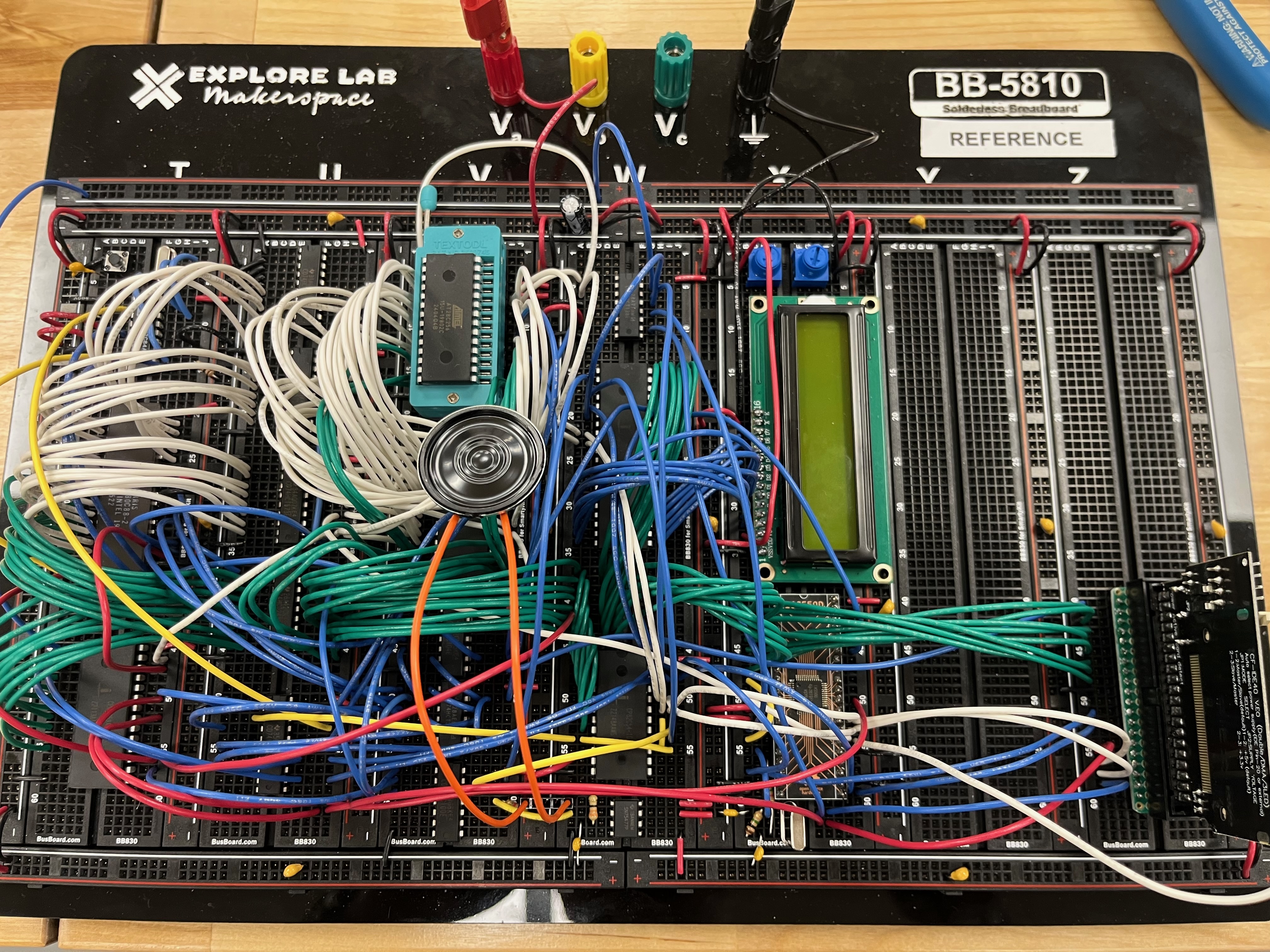
Step 5: Wire up the Speaker#
A PC speaker is a simple device that can be driven with a square wave signal. It combines a square wave with an on/off signal from the programmable I/O controller to generate sound or turn off.
Insert the SN74577P Peripheral Driver (U17) with pin 1 at W-60-E
Insert the Yellow-Purple-Red 4.7K resistor (R4) between V-60-J and VCC
Insert the Orange-Orange-Black 33 Ohm resistor (R5) between W-59-C and W-62-C
Insert the 0.01uf 103 ceramic capacitor (C4) between W-62-B and GND
Wire up power and ground
XS Black: W-63-A — GND
XS Red: W-60-J — VCC
XS Red: W-61-J — VCC
XS Red: W-63-J — VCC
XS Red: W-60-A — VCC
Wire up the clock signal wires (yellow):
S: V-60-I — W-61-A
M: V-59-J — W-53-I
Wire up the control signal wires (blue):
L: V-58-J — W-17-B
Plug in the speaker between W-59-A and VCC
The orientation does not matter
Warning
Someone who did not wire the breadboard should now verify the above steps were completed correctly.
Your updated computer should look like the following:
Test your work#
Power on your computer and confirm that it still displays the greeting from the previous lab. The red power LED on the CF adapter should be lit. You might be able to hear a slight pop from the speaker when you turn it on.
Lab Report
Take a picture of your breadboard.
Step 6: Get Ready for Boot#
Insert the Serial to USB adapter with pin 1 into Z-30-E
Note that pin 1 has a label of DTR and pin 6 is labeled GND
The pins might be difficult to insert; don’t force, but wiggle them until they go in
If there is a jumper on the adapter, remove it
Wire up the adapter
XS Black: Z-35-A — GND
M Blue: X-48-J — Z-34-A
L Green: X-49-B — Z-32-A
L Green: X-50-B — Z-31-A
Insert a CF card into the CompactFlash adapter
Wiggle the card a bit if the pins do not line up
Connect a USB cable from the Serial to USB adapter to your computer
Download a copy of
bios.binto your flash driveRemove the ROM chip from your computer by lifting the bar on the ZIF socket and removing the chip
Take your flash drive and ROM chip to the computer with the ROM programmer.
Insert the ROM chip into the programmer and the flash drive into the computer
From a terminal, run the following command:
minipro -p AT28C256 -uP -w /path/to/bios.bin
Replace
/path/to/bios.binwith the path to the file on your flash drive, which you can do by dragging the file into the terminal window.Once the command completes, remove the ROM chip from the programmer
Eject your flash drive from the computer by dragging its icon to the trash
Insert the ROM chip back into the ZIF socket on your computer and lower the bar
The next part of the setup depends on your operating system. Jump to the section that applies to you.
Windows#
Download and install PuTTY
Open Device Manager
Find the COM port for the USB adapter
It will be listed under Ports (COM & LPT)
It will be something like COM3 or COM4
Open PuTTY
Select Serial from the setup menu on the left
Set the Serial line to the COM port you found in Device Manager
Set the Speed to 9600
Set the Data bits to 8
Set the Stop bits to 1
Set the Parity to None
Set the Flow Control to RTS/CTS
Select Session from the setup menu on the left
Set the Connection type to Serial
Click Open
You should see a blank screen
When you want to exit, just close the window
Continue to the Booting section
MacOS#
Open a terminal
Install the picocom program using Homebrew:
brew install picocom
Run the following command to find the serial port for the USB adapter:
ls /dev/tty.usb*
It will be something like
/dev/tty.usbserial-XXXXRun the following command to open the serial port:
picocom -b 9600 -f h /dev/tty.usbserial-XXXX
You should see a bunch of setup information
When you wish to exit, press
Ctrl-AthenCtrl-XNote you may wish to run
resetafter quitting to reset the printing format in your terminalContinue to the Booting section
Step 7: Booting#
It’s time to boot! Turn on your power supply and observe the messages on the LCD Screen. Yous should first see “CRC Passed” to indicate that the BIOS has passed its self-verification. You should next see a message indicating the memory is being checked. If you see something else, it gives you an indicator of the circuitry to check. Note, that the memory check will also display on your computer. Once it is complete, the computer will try to boot from the CF Card.
Yous should see something akin to the following:
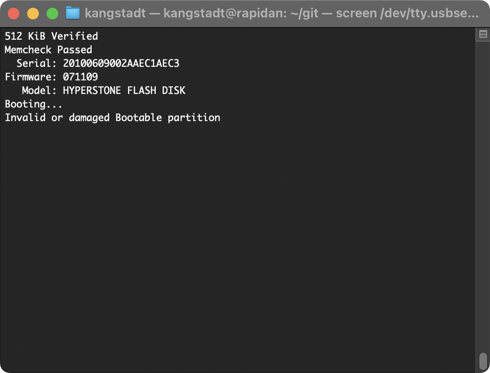
Congratulations! You have successfully built a computer that can boot from a disk! You can now run a simple operating system.
Lab Report
Take a video of your breadboard computer booting.
Note what happens if you press the reset button on the computer. Does it fully
perform the POST? Look at the
ARC86-BIOS to see if you can
find out how the behavior changes. Start looking in bios/bios.asm.
Lab Report
Explain your findings with the reset button.
Step 8: Lab Cleanup#
Before you leave, make sure to clean up your station. This includes:
Placing all leftover components back in the foam or in the bags
Coiling up the power wires and placing them by the power supply
Turning off the power supply
Leaving your station neat and tidy
Step 9: Lab Report#
Collect your notes into a well formatted report that details your progress through this lab assignment. Begin the report with a brief abstract that describes the purpose of this lab (in your own words) and what you were able to achieve.
In the remainder of the report, be sure to address the callouts throughout this lab description. When screenshots or images are requested, provide a brief caption describing what is being shown.